
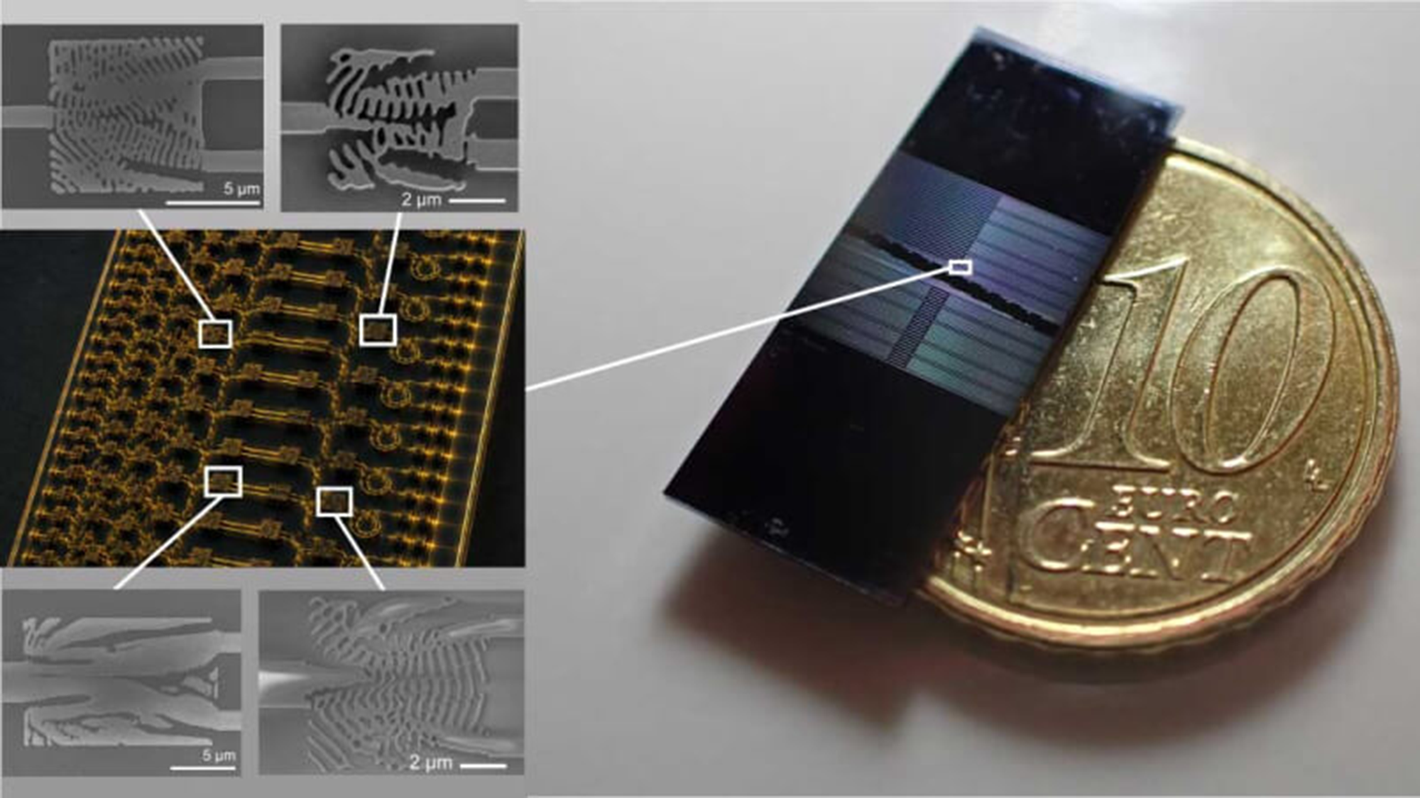
Researchers have achieved a significant breakthrough in photonic microchip design by using artificial intelligence to create components that are up to 500 times smaller than conventional engineering would allow. The study, published in Nature Communications, demonstrates how AI algorithms can generate nanostructures that push the boundaries of what was previously thought possible in chip miniaturization.
Photonic chips rely on light particles rather than electrons to transmit and process information, enabling faster data transmission and lower energy loss compared to traditional electronic chips. These devices are essential for fiber-optic communications, data centers, autonomous vehicles, and quantum computing applications. The three components shrunk in this study—wavelength splitters, spatial mode sorters, and mirrors—are crucial for directing and managing different light wavelengths within extremely tight spaces.
The AI algorithm employed an “inverse design” approach, working backward from desired performance specifications to generate novel geometric structures that human engineers would not have conceived. By defining what the light needed to accomplish and applying manufacturing constraints, the system created refined nanostructures capable of achieving the required results. The resulting components, fabricated from silicon nitride, demonstrated exceptional performance, with mirrors reflecting up to 98.5% of incoming light while being mere micrometers in length.
This advancement suggests that integrating AI into semiconductor design could unlock new possibilities for packing additional functionality onto photonic chips. While the components have been successfully demonstrated individually, researchers plan to combine them into fully integrated circuits as their next objective, potentially transforming the capabilities of photonic technology across multiple industries.
Originally reported by Livescience →
About the Author